Building a PICkit3 clone
I already own a PICkit2 clone for a while, and it worked without problems. But since it has been deprecated by Microchip for several years now, it doesn’t get any updates anymore. And so I found several times that it just doesn’t properly support the PIC chip I wanted to use. One can compile the pk2cmd application on Linux, to get at least programming support (it seems to be updated from time to time). But when used from MPLabX, only limited device support is available. And there is no PIC32 support at all.
So when I saw the updated QFP protoboard from Dangerousprototypes, I thought I might have a go on building my own PK3. The schematics for it are available from Microchip (in the user guide), and the needed firmware can be found in the PICkit3 scripting tool package. So I spent my Free PCB coupon on this board, and started another project.
I had most of the needed components available, and got the MCU via Microchips sample program. While waiting for it to be delivered, I took the schematic and replicated it in KiCAD. While doing so, I found some more components I had not available, and replaced them by an equivalent solution.
Some circuit redesign
In the end I replaced basically the whole circuit related to handling switching the voltages to the output. In the original circuit this is done by discrete transistors (FETs mostly, including two combined in a single package). Instead I used a LTC4411 ideal diode and a MAX893L high-side load switch. The LTC4411 is not just a diode with low losses, but can also be used as switch. So it was ideal for switching the power coming from the USB power rail, because it can handle high enough currents and is reverse-protected (so no current flows into the USB port when it gets powered off and the connected device is still powered). The low losses mean that the circuit gets the voltage as its on the USB bus, and not something lower. The MAX893L then switches the power rail for the target MCU (when its powered by the PK3). Its current limit is configured to 500 mA, so the USB power is not overloaded.
I also exchanged some transistors with equivalent ones I had available, and replaced the bi-color LED with two single ones. This makes the color codes explained in the PK3 user manual invalid, so I added a small table on the case to know what the LEDs mean (see below).
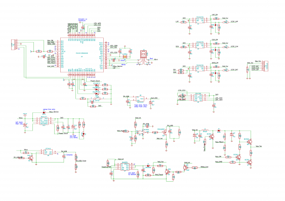
Here is the full schematic in all its glory:
On the top left is the MCU with all its supporting circuitry. To the right are the voltage level translators and the outgoing ICSP header. below the MCU is the 3.3 V regulator for the MCU power rail, and the USB power switch. Further to the right we find the MCP1525 voltage reference, used for measuring the generated (or provided) voltages. Then comes the target voltage regulator - an OpAmp driven by a PWM signal, using a FET for regulating the output. Right at the bottom there is then the power switch for the target voltage. On the bottom right is then the switch-mode converter for generating the programming voltage.
First test
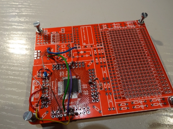
When the MCU finally arrived, I started my work by making sure the MCU runs on the protoboard at all. So I soldered it down (drag-soldering, enough flux and some solder wick), together with the support circuitry (mainly just the decoupling caps and crystal):
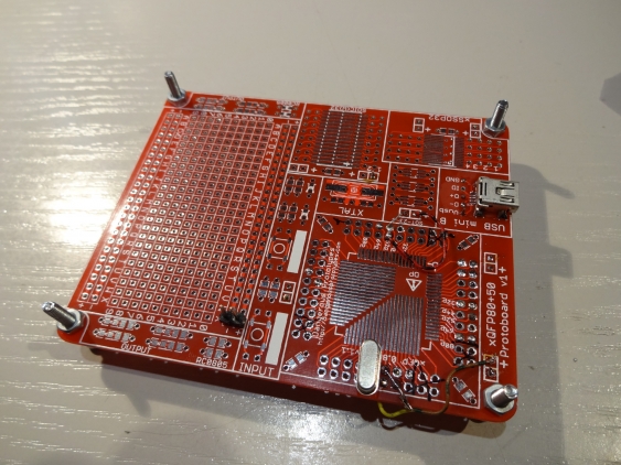
The side with the MCU would later become the bottom. This is because the protoboard has two different footprints for QFP packages, in different pitches. Since the MCU comes in 0.5 mm pin pitch, it needs to go to one side - but all the footprints for the SMD ICs are on the other side. So the bottom side gets the MCU (and some caps), and aside from that just most of the wiring. The top side for now has only the crystal and the USB connector on it:
Having build the basic MCU circuit, I added a (temporary) ICSP header to the MCU pins, connected it to my PICkit2 and programmed the firmware for the PICkit3 (fortunately the MCU is supported by the pk2cmd application). When I then connected it to the PC, it got recognized as PICkit3. Huzzah! First hurdle taken…
Building the complete the PICkit3 circuit
So I went on adding all the remaining components. Doing so turned out to be more tedious that I thought. One needs to plan ahead with regards to placing the components, to be able to use short connections. I placed multiple ICs on the single SO-28 footprint, so I needed to always lookup which pin is in which location. And the header pins for all most of the footprints are not in a single row, making counting even more difficult. Its really easy to make a mistake that way.
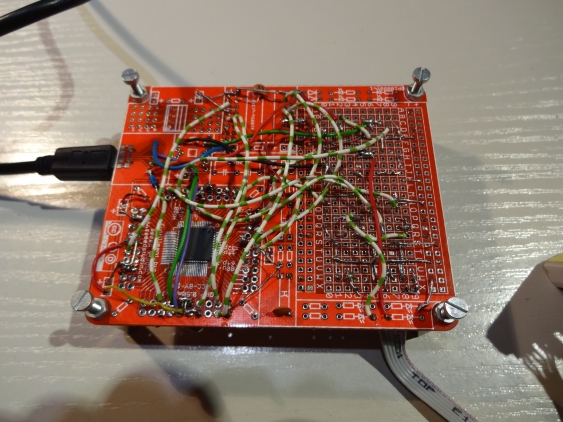
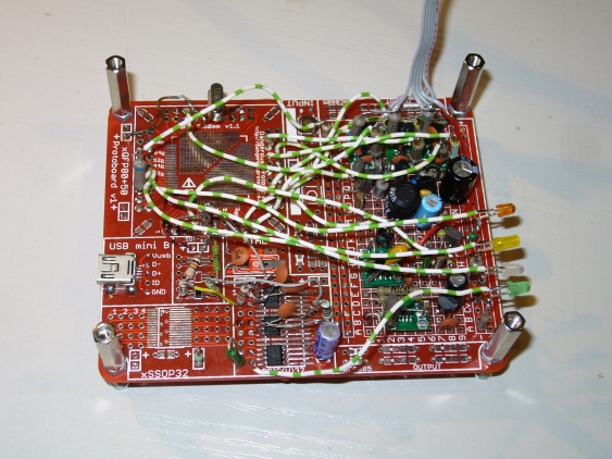
So I took my time for that, doing only one part of the circuit in one session. That meant it took many evening to get it finished, but its better not to rush it. Finally it look like this:
On the bottom there is still only the MCU mounted, but now a fair bit of wiring is there too. On the prototyping area part I used mostly short bare wires, so this is a little bit hard to see. For this part of the wiring I carefully planned the placement of the components, so I needed only a few normal wires. The one lone capacitor in the lower area is attached to a push button on the other side.
The top side contains all the other components, so it looks much more crowded. The wires seen here are needed because the parts they are attached have no connection to the board. The LEDs as shown here got later moved to the enclosure. The other wires are connected to resistors on the level shifters, which I mounted on small SOT-23 breakouts.
One can see that I still used some SMD breakout boards, instead of using all the available footprints on the protoboard. This is because their placement was not optimal for me. I used three level shifters in SOT-23, but the SOT-23 footprints are in the middle of the boards, and the ISCP output header should be at the board edge. (And even then there would have been two SOT-23 components left). The LTC4411 should go near to where all the power switching happens, so it went to the perfboard area too. (Together with the MAX893L, for the same reason).
The three SO-8 chips on the SOIC28 footprint are (from bottom to top): the MCP1727 voltage regulator, then the 25LC256 EEPROM and the MCP601 OpAmp. The latter one is located closely to the PMV48XP FET on the SOT-23 footprint to its left).
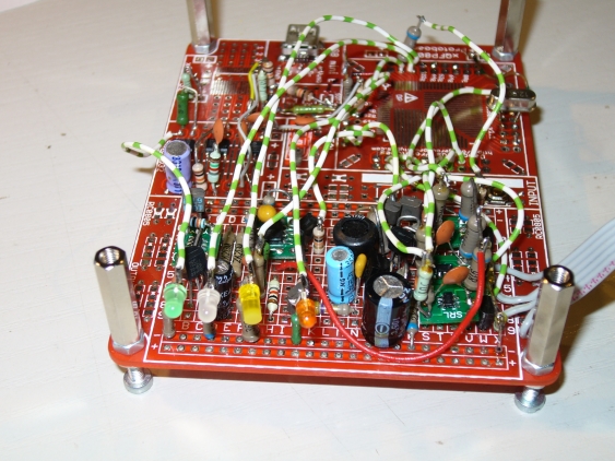
On the prototyping area, the bottom parts are the MAX893L and the LTC4411 used for switching power. They go with some transistors (to negate the logic signals). In the middle part is the boost converter for the programming voltage. It’s quite crowded there, but I wanted to get as short connections as possible (and additionally there wasn’t so much space left - planning was a little bit bad). On the top are the three level converters (74LVC1T45) for the ICSP target connection, each together with its support circuitry on a breakout board of its own.
The stuff on the prototyping area can be seen better from the side:
First tests
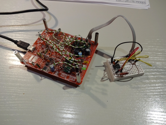
Having finished the build, I connected the ISCP header with a short cable, and tested it with a PIC12F1822 on a breadboard:
And thats where the problems began… I was able to successfully detect, read and write the PIC with the PICkit3 scripting tool (using a VirtualBox VM with Windows in it - doesn’t run on Linux). But using it with MPLabX did not work properly. The PK3 got detected, a new firmware got uploaded (as it should), but then MPLabX told me that it didn’t like the firmware it just uploaded:
Connecting to MPLAB PICkit 3...
Firmware Suite Version.....00.00.00
Firmware type..............Enhanced Midrange

Downloading Firmware...
Downloading bootloader
Bootloader download complete
Programming download...
Downloading RS...
RS download complete
Programming download...
Downloading AP...
AP download complete
Programming download...
Your PICkit 3 firmware version is too old. You must have firmware version 00.00.00 or higher to use MPLAB X.
Connection Failed.
Really strange. Since using the standalone GUI did work properly, I was sure that the PK3 worked properly (it actually did from the beginning, there were no problems whatsoever). So I suspected there might firmware issues. But tests with the older MPLabX (1.70), on Windows XP or even the old MPLab 8.91 yielded the same error. After a long search, and leaving the project laying on my bench for about a month, I finally had an idea.
Somehow, so I thought, there must be a difference in how the scripting tool and MPLabX use the PICkit. One difference I could imagine is that the scripting tool uses always the same firmware, whereas MPLabX changes parts of it depending on the type of PIC used. And this firmware gets stored in the EEPROM… So I attached a logic probe (a home-made one, should make a post about it…) to the EEPROM signals and then used both programs. It turned out that the scripting tool doesn’t use the EEPROM at all, whereas MPLabX tries to access it. So I verified my wiring with the schematic - everything was OK. But when I then compared my version of the schematic with the original one from Microchip, I found the error - a really stupid one:
The EEPROM is connected via SPI to the MCU (together with the second used to the on-the-go function, which I didn’t place). For this connection two data lines are used: SDI and SDO (serial data in / out), together with clock and chip-select. In my schematic, I connected SDI on the EEPROM with the SDI line on the MCU - after all the signal is named the same. But that was wrong - in the original circuit, on both the EEPROM and the MCU the signals are named as seen by the respective component (so both see ‘SDI’ as an input). That meant that SDI on the MCU needed to be connected to SDO on the EEPROM, and vice versa. So I just swapped the two wires, and everything worked as expected.
Finalizing the PICkit3 clone
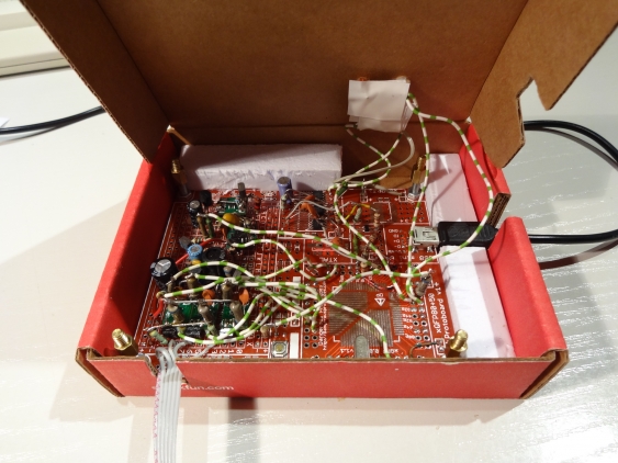
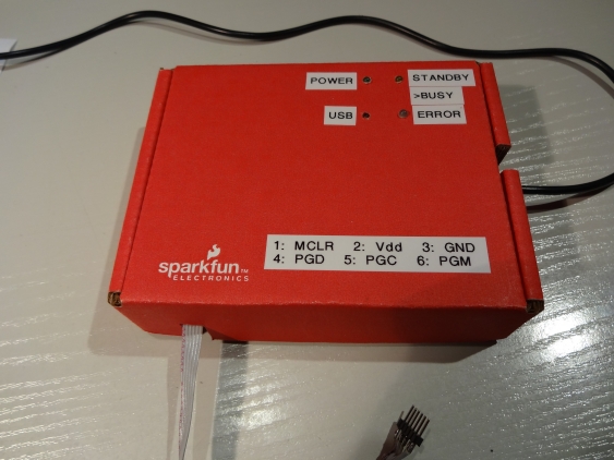
Having solved that last problem, I went ahead and looked for an enclosure. Finally I found a Sparkfun box, where the board fitted nearly perfect in:
I used 30 mm M3 screws as standoffs, and prolonged them with some small PC main-board standoffs - together they had the perfect length.
The I removed the LEDs from the board, and fitted them into the enclosure. The two LEDs forming the dual-color one from the original went together, and I added labels for everything. I also added a label with the ICSP pin-out, since I can never remember it:
It looks like the PICkit2 I build earlier last year, but the fourth LED gives it away…
So now I’m fully equipped for working with all the PIC chips from Microchip, even including the PIC32. Being able to really debug them is a great step forward than just uploading a program (though one can get used to debug a program by just looking hard enough at the source code…)
Experiences with the protoboard
So what is the final verdict on the protoboard? After all, I could use it to build a rather complicated project on it, so it has proven usable. I like that it has a large number of different footprints and connection options available.
But if they are not used, they are just in the way. I did not use the SSOP footprint, and it takes much room. The footprint for the crystal was on the wrong side of the QFP footprint for me (one needs to be lucky to have it at the right place).
Having the footprints for the push buttons in the middle of the board means they are most likely covered by wires. So maybe they should go further to the edges. This would also move the prototyping area more closely to the QFP footprint. Maybe it should go to the center, with all the other stuff around it. There might also be space to save by not using through hole connections for all parts. Maybe just using SMD pads for connecting wires to the crystal can reduce the overall footprint in half, without sacrificing usability.
One thing constantly ticking me off is that the numbering on the QFP footprint differs by side. Since the MCU comes in 0.5 mm pitch (as do most QFP parts I found) it goes to the bottom side of the PCB, whereas anything else goes to top. But there the layout is reversed, so I needed to avoid looking at the QFP pin numbers and always needed to count in reverse. Thats really annoying. Next time I would rather use the single-footprint version of the board just for that reason (even if it comes without USB footprint).
I liked the availability of a 3.3 V power rail in all the different places around the board. But since the PICkit uses different voltages (3.3V in some places, and a switched voltage rail called VDDint in other places) I could have used a second voltage rail. I suppose the same might be true for other projects, needing 5 V and 3.3 V.
