« Unboxing the Wireless power demo kit - first impressions
| Main |Measuring the performance of the wireless power demo kit »
AXP1G57 configurable logic demo board - first impressions
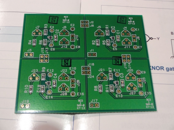
So the evaluation board from NXP has arrived safely. Its larger than I expected (about 7.5 by 6 cm) - because its four boards in one:
Each of the four parts of the board contains a single 74AXP1G57 chip (the really small blob in the middle), surrounded by connectors to all pins, and the needed passive components (and even some more).
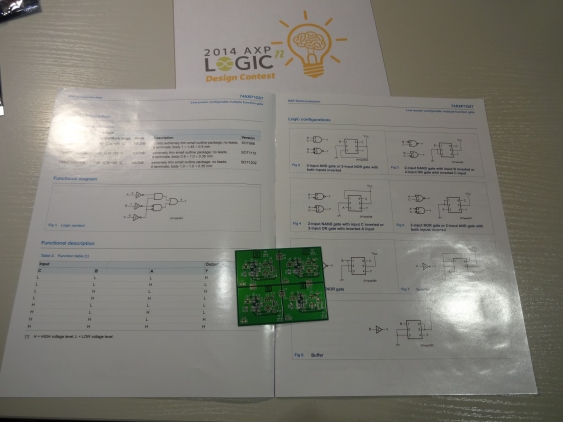
Also in the package was a foldout outlining all the different logic functions, how they work and especially how they are configured. (Each function has a different input connected to either ground, Vcc or another pin).
Using as a breakout board
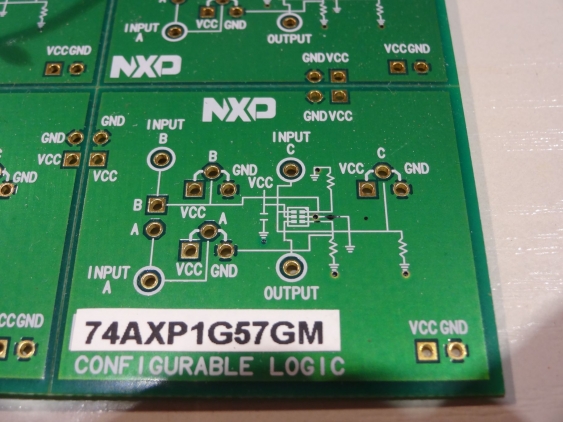
While the board is promoted as ‘demo board’, I intend to use it more as a breakout board for the 1G57 chip. For a demo board, it does a really good job. The chip with its different connections is printed on the silk-screen (as a real schematic), and this also shows the passive components. The connectors are all logically ordered, and there are even multiple pins available for the inputs. This allows adding fixed connections of the inputs to either ground or Vcc, or to bridge the inputs together:
This allows for easy configuration of the different logic functions available with the 1G57. It would have been nice, though, if NXP had included some header pins. I can understand they are not mounted - the board is so flat it fitted nicely into a letter envelope. For connecting different pins together one can place small wire bridges on the pins. Since one need the soldering iron anyway, adding solder bridge pads additionally would make that easier..
Another nuisance is that the four single boards, when separated (they are V-grooved), cannot be stacked easily. When looking at the single board, one sees that the ‘global’ Vcc and ground pins are not located in the same positions between the different boards. They are always at the inner borders, but that means they don’t match up when stacking the boards on top of each other. Only the bottom-right ones match up.
So I reckon its not so good as a breakout - the usability when trying to integrate the board into a surrounding circuit its not the best. But it was not designed as such, so I cannot hold this against it. And thats one of the charms of this contest for me - using what I’m giving in a way not really intended.
Testing with a first circuit
OK, time for some real tests. Since I needed a square wave signal anyway for my project, the first test I made was just using one of the gates as a NOT gate to create a simple RC oscillator.
Building this was simple and effortless. The multitude of pads around the chip left enough place to add all the components (OK, there were just two of them…).
Unfortunately, after powering up it didn’t work. I just got a steady ‘high’ signal on the output. So it got time for some debugging. After checking all the connections and the soldering, I remembered that there were not only the decoupling caps on the board, but also some resistors. Time to check the schematic from the silkscreen.
And there it was - the input from the gate had a 4.7 k pull-down resistor on it, and the feedback resistor for my RC oscillator was 82 k. So the input was low all the time… After removing the offending resistor, everything was fine.
Future plans
So after this first go on the demo board, its time to go into deeper planning. Next time I will report how I plan everything to work. Its rather interesting what one can do with just four little logic gates and some discretes…


