Wireless Power - the full schematic explained
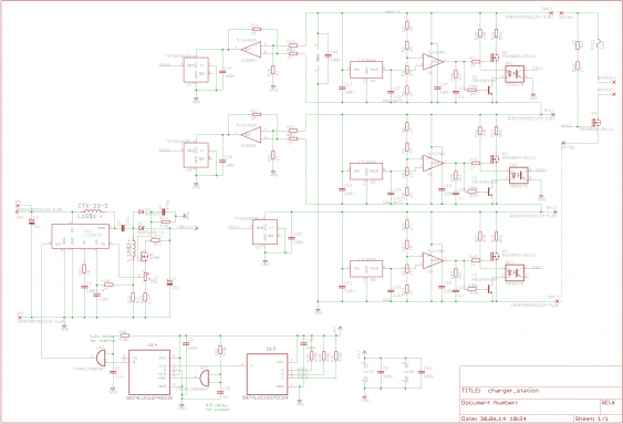
Since the contest is now nearing its completion, I gather its about time to actually show and explain the whole circuit. I already went through some of the parts of it, and how I decided how to build it. But I never showed how these parts work together. So lets have a look.
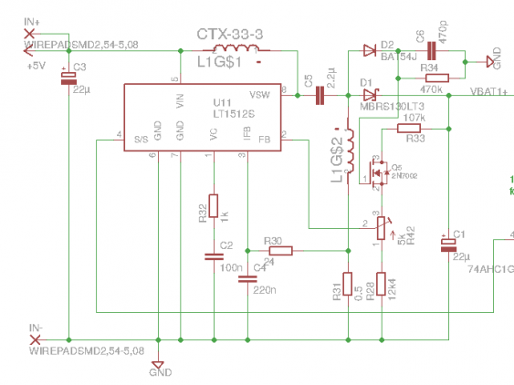
Lets start where the power comes in. The wireless power receiver delivers 5 V, which are connected to the 5 V rail in the bottom left. There it powers the DC/DC converter:
This boost converter not only creates the up to 12.6 V needed for charging the battery pack. It also handles the current limiting needed for charging. So the charging follows the CC/CV profile needed for LiIon batteries.
This part of the circuit is directly from the LT1512 data sheet. The feedback resistor divider (R33 + R28) has been selected to have an end-of-charge voltage of about 12.3 V. To handle the possible inaccuracies of the LT1512 reference voltage, it can be fine-tuned with R42.
The combination of Q5 and D2 disconnect the feedback divider from the battery when the charging has stopped (and the input voltage gets disconnected). This is needed because otherwise it would draw a significant current (and the data sheet explicitly states that the values cannot be made larger).
Noteworthy is the use of a dual coil with coupled windings. They are needed because the converter runs in SEPIC configuration. This makes the PCB design a little bit more difficult because now the orientation of the single windings matter.
The output of the converter is connected directly to the battery pack, so it can correctly sense the charging current and the current voltage. That leads us to the cell balancers:
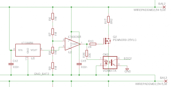
There are three of them, but they are all the same. On the left is the LTC6656 voltage reference, delivering 2.048 V (with 0.05% accuracy and 10 ppm °C temperature drift) with just 1 µA. The battery voltage is exactly halfed (by R6-R9), so the balancing voltage is 4.096 V. The divider is made by four 1M resistors, since Farnell had not 2M resistors with 0.1% accuracy available.
For handling the shunt current for balancing, a N-channel FET is used. So the OpAmp (a LT6003 low-power amp one with also a low input bias current and low offset voltage) drives it to draw so much current that the voltage on the cell is equal to the end-of-charge voltage. As soon as that happens, the opto-coupler will also turn on. Since the gate-threshold value of the FET is higher than the voltage for the LED inside of the coupler, this should result in a sharp turn-on.
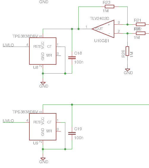
Each cell is not only connected to its balancer, but also to the comparator used for the under-voltage-lockout. The two upper cells are not connected directly. Instead, their voltage is taken by a difference amplifier, that changes the cell voltage to be ground-referenced. Only then the comparator can detected the low-voltage situation. The TLV2402 used here is also a low-power type, and its inputs can exceed its power rails, making it ideal for this situation.
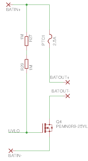
Since the TPS3838 comparators have an open-drain output, they can be connected together directly. When one cell voltage goes too low, the output will be switched to ground. This will then turn of the FET that normally connects the battery pack to the output. This FET is enabled by a large resistor pulling its gate to a positive voltage.
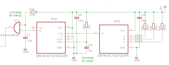
The last part is the end-of-charge detection. For that, the output of the three opto-coupler (driven by the balancer) are connected to a NOR gate. That means as long as at least one cell is not in balancing mode (so its EOC signal ist still 1), the output of this gate is 0. When all cells are in balancing, this output goes to 1. This change is the used as clock signal to the D-Flip-Flop, which then transfers the 0 from its data input to the output. This 0, in turn, disables the DC/DC converter.
The AND gate (an AHC1G08) is used to delay the startup of the converter for about 1 second after the wireless power receiver turns on. This allows for a little improvement of transfer range - the distances during startup are larger with less load. The D-Flip-Flop gets pre-set (to 1) with the small RC-combination R43/C21. Since the DFF expects fast-rising signals, the time constant here is rather small (less than 10 ns).
