« Building a multi-voltage reference for my DMMs
| Main |Wireless Power - the full schematic explained »
wireless power - status update
So the last couple of weeks was silent with regards to my project - I was just too busy. Being on a business trip left not so much time for doing electronic projects (and I forgot to take the Eagle project with me). And the aftermath was then rather busy at work.
But I got new transmitter coils from Würth in the mean time, and did some experiments with them (which need a write-up).
Apart from that I have finalized my schematic, and added all the missing details I already explained the most important parts of it, but there are still some minor tweaks here and there. So there will be a separate post about it.
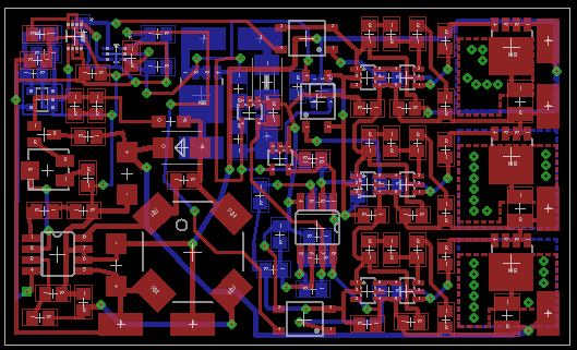
Right now I’m busy getting the PCB done. Since I’m rather space limited, I have just 65 by 40 mm PCB area. In that space I need to fit three balancers, the UVLO circuit and the charging circuit. So this will be densest board I ever layed out. I’m using a 10 mil grid with tracks down to 12 right now (and it seems I can place and route everything with that). So there is no chance to draw this manually as I did in the past (I switched for some ICs to the 0.5 mm pitch version just to save space, thought the passives are still 0805). So it will probably go off to a PCB prototype manufacturer, which also needs some time.
Its a pity that the Farnell coupon cannot be used for the PCB manufacturing. Having it manufactured in Europe can get quite expensive. WEDirekt could do it in 5 days for 74 EUR. EuroCircuits (the Farnell partner) would charge me 45 EUR, but would need 7 working days (and the express shipping costs another 10 EUR on top). In contrast, having it manufactured at SeedStudio or ITead costs 15 USD for 10 boards - but then the shipping is another 25 (DHL) or 35 (UPS) USD (doing the normal shipping means waiting three or four weeks)
Speaking of the PCB: For several parts of the PCB I did multiple routing passes to get a good layout (which means ripping up all the traces, re-orientating the components and do a re-route). For the charger, I used the recommended layout from the LT1512 data sheet, which is quite compact. Unfortunately its not very compact - the coil alone takes significant board space. The most difficult part were the balancers, since they should be all beneath each other. It took me three iterations to get it right. Looks like I found a design in the end that is small, looks quite good and allows for some thermal relief for the balancing load FETs.
I managed to route anything, but I really need to clean up all the traces. Shuffling around the components always moves them around so they look quite messy now. The top side is nearly completely populated with parts, and the bottom side to about its half. I did not even found a place where to put some mounting holes, so I need to live with some rubber feet.
Its probably not the best layout, but all the critical parts should be OK.
