Stairstep generator with a PSoC4
A while ago I ran across this video from w2aew where he explained using two generators and an integrator to form a stair-step generator. I was intrigued because it seemed like such a simple idea, and a useful one too, but I immediately thought of some improvements. First I wondered why he didn’t implement both generators with 555 timers, and second a voltage buffer on the output seems to be needed.
But then my mind wandered and I realized that the two oscillators were actually PWM generators. And then I it was only a small step to “this can be implemented in a PSoC much better”. So I went ahead and tried it.
How does the stair-step generator work?
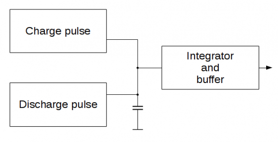
The generator as presented by w2aew consists of three main build blocks:
- a pulse generator used for charging a capacitor up step by step
- a second pulse generator used for discharging this capacitor again
- and a Deboo integrator which ensures the charging of the capacitor is linear over time
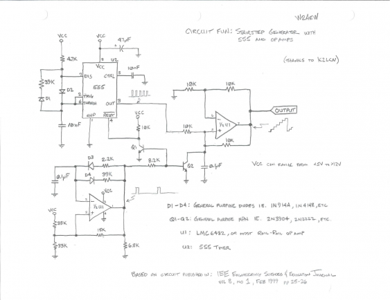
The detailed circuit:
is a little bit more complicated - so for a detailed explanation just watch w2aew’s video. He explains very nicely how this circuit works in detail. To understand how I implemented it in the PSoC4, here is the short version (using the block diagram from above):
Each positive pulse by the ‘charge’ PWM charges the capacitor by a small amount (the Deboo integrator ensures that this happens linear over time). When this PWM goes back to ground the integrator just holds the current voltage level (because both inputs are connected to a 1:1 resistor divider then). As a result we get a step-by-step waveform. When the second PWM creates a pulse (connecting the capacitor to ground) it discharges the capacitor, so the output goes back to zero. After that it starts again by getting the capacitor charged from the first PWM. Both PWM generators need to be synchronized so that the charging pulses start at a constant time after the discharge pulse.
Maxim has a quite detailed explanation of how the Deboo integrator works. In short, its a current source that charges a capacitive load. With the input charging resistor connected to the positive rail, the capacitor is charged. Connected to the negative rail its not discharged, but the voltage is held at the current voltage level.
So how can we implement this in a PSoC?
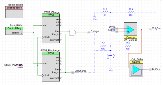
I wanted to use one the the small CY8CKIT-049-42xx prototype boards, which comes with a PSoC4 4200 series chip. This PSoC4 has multiple TCPWM blocks that can be used as PWM, as well as two OpAmps which can work up to 6 MHz. So apart from the passive components everything we need is on board. So we can just take the block diagram and draw it in PSoC Creator:
The upper PWM block is configured with a period of 100 clock cycles and a pulse width of 2. The lower PWM runs with a period of 1000 clock cycles and a pulse of 80 cycles. I’m using the negated output, so its high most of the time and goes low only during the discharge. This signal is also used to disable the charge pulse during discharge, by using an AND gate (its not actually needed, but makes the discharge faster). The outputs of both PWMs are then routed to pins of the PSoC. The ‘Charge’ pin is configured as push-pull. In contrast the ‘Discharge’ pin is configured as ‘open drain, pull low’ output. So its open as long as the signal is high (so it doesn’t affect the signal), and only goes to ground if the signal goes low (discharging the capacitor).
Since the two PWM periods are synchronized already (giving 9 stair steps) they just need to be started at the same time. This is accomplished by an internal start signal, created by a control register.
The first of the two OpAmps is configured as normal amplifier. The blue lines indicate external connections, that are not routed inside of the PSoC. There is one caveat here: one of the dedicated OpAmp pins is connected to the board LED. So this pin cannot be used. Therefore I did assign the pins for the first OpAmp manually to avoid this pin (it one of the positive inputs). The output of the integrator is brought to a pin (for connecting the resistors), and routed internally to the second OpAmp. This internal connection avoids usage of the dedicated pin, so we avoid the LED. This OpAmp is configured as simple follower, so it acts as a buffer.
Build and test
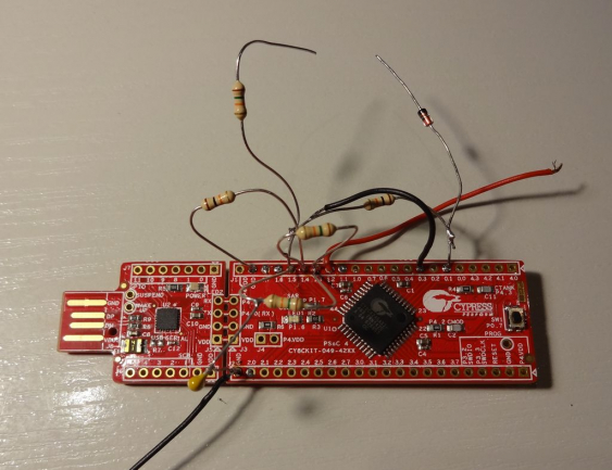
I used one of the small CY8CKIT-049-42xx kits to build my test circuit:
The left part of the PCB is the USB_UART bridge thats used for bootloader programming. The right side is the actual PSoC4 board. I just soldered the passive components onto the provided header pins. On the upper part I added the additional diode and the resistor to get higher amplitudes. They are not soldered together so I can test both versions. The red wire is the output.
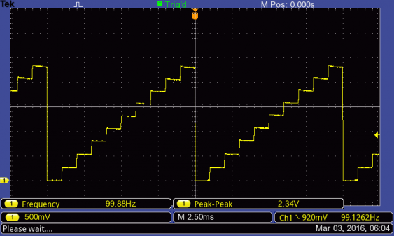
Since the PWM clock is 100kHz, and the period of the reset PWM is 1000, the output is a 100 Hz waveform (with a step frequency of 1 kHz). The resulting waveform looks quite good:
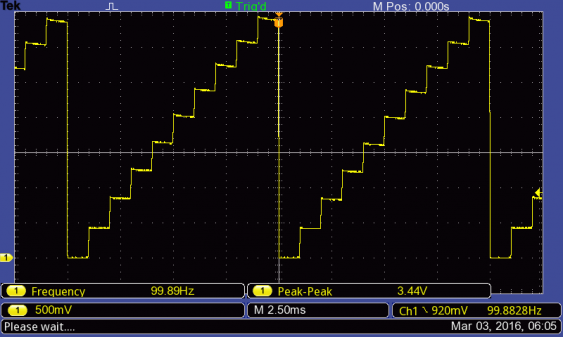
The amplitude is about half of the supply voltage. To increase it, all four resistors would need to be changed, to keep the integrator in balance. But an easier way is to reduce the value of R_1, but only when the capacitor is charged. To do so, I added a series combination of a diode and another 10k resistor in parallel to R_1. The result is an increased amplitude:
When the amplitude should be variable, then either the buffer should be an amplifier with variable gain, or a potentiometer needs to be added to change the attenuation.
By changing the PWM periods the frequency can be higher or lower, as long as
- the period of PWM_Reset is 10 times the period of PWM_Charge (otherwise the PWMs are out of sync)
- the pulse width of PWM_Charge stays constant (since it determines the step height)
- the pulse width of PWM_Reset is a little bit lower than the period of PWM_Charge
When the input clock is increased, the pulse width of PWM_Charge need to be adjusted so the charge pulse has the same height. For even higher frequency the parallel resistor
Since the OpAmps are able to handle up to 6 MHz, the output frequency can be quite high. Its still quite accurate - the internal oscillator of the PSoC4 4200 series is specified with 2% accuracy.
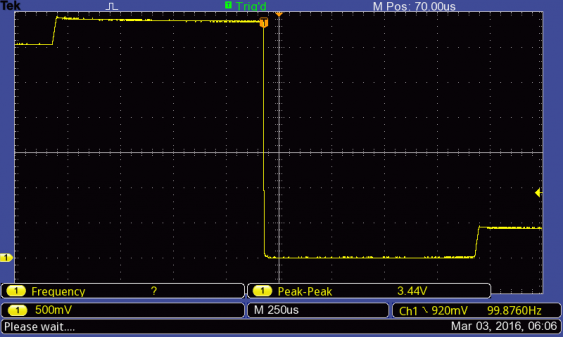
When zooming in on the waveform:
the rise time for each step can be estimated - its about 25 µs. But we can also see that in the steps with a higher voltage level the voltage drops a little bit instead of staying constant. This is probably because the two resistor dividers are not exactly equal which results in either a slight discharge (when the inverting input is at a lower voltage than the non-inverting) or a slight charge (when its the other way round). This could be solved by adding a potentiometer to the fixed divider.
Outlook
We have seen how useful a chip is that has really configurable hardware inside. Being able to start two PWM exactly synchronized, gating one of the outputs with the other one and having configurable OpAmps can make for really simple solutions.
So thats it for today. I will do some investigation in increasing the frequency, and making the rise times shorter (by using a lower value resistor for charging). Also the steps should be flat, so I need some adjustment for the resistor dividers.
Then I plan to extend that generator a little bit with additional. With the PSoC4 capabilities it should be easy to also get a downwards stair step waveform, and also an up-down waveform. All of this should be able to be handled in hardware (though some software would be needed to reconfigure it on-the-fly). This will be a nice show-case for why I like to work with PSoC chips - they make so many features so easy to implement.
