Building the LogicBoost free PCB
After finishing my last free PCB build I got a new coupon from Dangerous Prototypes. Since the free PCB drawer over at DP is sometimes empty, it took a while to find something interesting. But finally a PCB for the MSP430 variant of the Logic Shrimp logic analyzer, called the LogicBoost, arrived there. It is a 6-channel logic analyzer with 20 MHz sample rate and 256k samples. So I ordered one, and it arrived yesterday. The only component I needed was a ‘573 octal latch, which I ordered in advance.
So when the PCB arrived, I was ready to go. Soldering took about half hour or so, and went without problems. For finding out which components are really needed I went with the screen-shots from the DP forum - there is no other documentation available right now. (One can spare C8 and bridge R1, and the resistor network RN1 is only needed when the inputs are unstable).
I placed a female header for the probes, so I can use jumper wires to directly connect it to a breadboard. It also makes it difficult to accidentally short the pins when working with it. (I found it surprising that Vcc is no one of the outer pins as GND is - the AUX pin is located there) On the PCB itself there are no descriptions which header server which purpose (there is also a FTDI header so you need to look this up in the schematic). Also, there are no marks for how to place the board into the launchpad (the TI booster boards all feature a rocket icon which lines up with the icon on the launchpad itself).
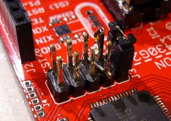
After downloading the firmware package I compiled the source and programmed it onto the MSP430 (and on the way discovered that I had an old installation of mspgcc lying around whose mspdebug didn’t know about the MSP430G2553). Everything powered up - but the OLS client was not able to connect to the LogicBoost. After a while I found out that the MSP430G2553 uses a hardware UART, and my version of the launchpad (1.4) needs swapped RX and TX lines since the pin-out has changed. Since there is no space left between the launchpad and the logic boost, I soldered the cross-connections directly onto the header:
So if you have a launchpad version older than 1.5, and don’t use the FTDI connector, you need to swap these lines too (and on launchpad 1.5 you need to set the jumpers properly).
After that, the OLS client found the LogicBoost, and was able to capture. But with the meager 9600 baud connection the launchpad UART-to-USB bridge provides anything above 1k sample size takes rather long to download. So I will build a USB-to-UART bridge next (I have a MCP2200 in my parts bin which should be OK), and will use it for powering the board too. Unfortunately the FTDI header doesn’t have a pin for Vcc, it only provides RX, TX and GND. So I need some cable soldered on instead of a nice connector.
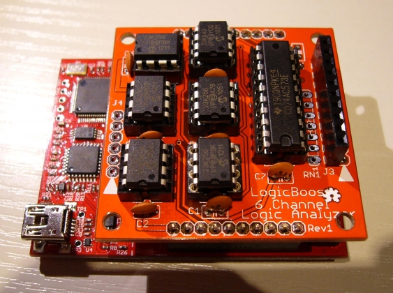
Last but no least a picture of the final board:
I used a 74AC573 instead of the AHC (or LVC) version. Since this version doesn’t handle input voltages above its supply voltage (at least no without current limiting resistors) this means I can use it only for 3.3V systems. But since most of my projects are 3.3V anyways I consider this OK. And I can add a resistor array later on as a flying connector anyways…

