« How to design a "most useless machine" with some logic gates
| Main |Two times is not enough - Measuring the performance of the wireless power demo kit part 3 »
Wireless power contest - strategies for charging a battery pack, part 3
In the first two parts of my wire less power contest series I had a look at options how to handle the charging of a battery pack. Either by dividing it into single cells or using a cell balancing solution. But I always supposed that there is a charge controller doing the important part of controlling charge current and end-of-charge termination. Now its time to look at this piece of the puzzle.
Just to recall: I’m using a battery pack made of three cells (so its nominal voltage is 11.1 V and the end-of-charge voltage at 12.6 V). The wireless power receiver delivers a voltage of 5 V, with a maximum current of about one amp.
Buck and boost
Since the input voltage for the charging circuit is smaller than the needed charge voltage, I either need to charge the cells each one on its own, or to convert into a higher voltage. I already ruled out the first option, since it will be too large and too inefficient.
So this means converting the voltage from the wireless power receiver into a higher voltage suitable for charging the pack. This again leaves two choices (probably this whole mess can be converted into a nice decision tree…):
- using a boost converter to create about 13 V and then use a dedicated LiIon charger
- use a LiIon charger capable of doing the boost convert by itself
At the first glance, the first option seems to be the better one: there are many DC/DC boost converters available, and also a good amount of LiIon chargers. But on a deeper look it doesn’t look so good anymore. When looking at TIs selection of LiIon battery chargers lists 200 ICs. Selecting 2-4 cells reduced it to 46, LiIon and a an adjustable voltage to 26. Most of them are in VQFN package only (and two in SSOP), leaving only 4. When looking deeper at them (the BQ2000 ,BQ2000T ,BQ2054 and the BQ2954) one discovers that they all are switch mode charger controllers. That means they need an external switch mode buck converter, which they control to regulate charge current and voltage. This makes them rather complicated and large (remember, I already need a switch mode boost converter). Also, doing two switch mode conversion in sequence might not be the most efficient method after all.
No boost needed
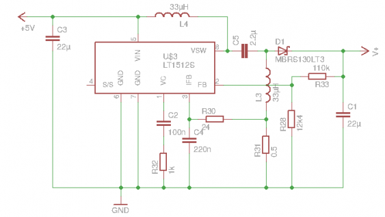
Looking at manufacturers like Linear Technologies, Analog Devices, STM, Fairchild or OnSemi doesn’t look better. So I went looking whether there might be a charger that can do the boost conversion all by itself. And lo and behold, I found not one, but two: the LT1512 and LT1513. Both are of the same family, and differ mostly in the charge current they can handle (0.75 vs. 1 A). But even they do not come without drawbacks: since these chips are designed as multi-chemistry chargers, they lack the charge termination handling for LiIon batteries. For that the LTC1729 is recommended, but its only usable for two cells (and not three). So I need to add that as well. Overall, using a LT1512 (which comes in 8-pin SOIC package) still results in a rather low component count. Since I need a balancing circuit for each cell anyway, I can handle the charge termination that way.
When one of the balancers starts shunting away current from the cell, I can use the output signal (driving the FET) to light up the LED of a optocoupler (similar to the solution used for the simple balancer). When all three balancers are active, the charge can be terminated. The capacity reached at that point is not 100 % (for that, a constant voltage charge with reducing currents would need to done). But with a charge termination voltage of 4.1 V a capacity of about 85 % can be reached (and about 90 % at 4.2 V). This is not too bad for such a simple solution.
It needs a little bit more components than the easiest boost converters, but overall its not that much: R28+R33 are the feedback voltage divider (configured for 4.15 V per cell), R31 is the current feedback shunt (for 200 mA), with R30 / C4 as lowpass filter. The rest forms a SEPIC-converter. Charge termination is controlled via the S/S pin (sync/shutdown), which is not connected when unused.
What’s left now?
So whats missing now for the complete picture? As already mentioned, the charge termination. I’m not sure as of now how to design it best. Maybe I can just put the three optocouplers in series, for form an AND gate. maybe some real logic is needed. I also mentioned already that a startup delay might be helpful. And last but not least I would like to use the Qi feature of signaling the transmitter that the receiver has finished loading, so it can tell this properly to the user. All of this together might warrant using a small MCU. We will see what comes up in the end.
Outlook
Since I got a load of new coils from Wuerth, the next post most probably will be about another round of measurements. I also started on looking at how to do the mechanical construction - it will be a though fit to get all of the needed stuff into the available space. And I already got the first parts delivered, so there is something to talk about that as well. Stay tuned!
